

Thin Film Substrates
- Products
- Deposition Materials
- Refractory Metals
- Rare Earth Materials
- Powder
- Technical Ceramics
- Lanthanum Hexaboride (LaB6) Materials
- Pyrolytic Boron Nitride (PBN) Products
- Boron Nitride (BN) Products
- Alumina Ceramics (Al2O3)
- Aluminum Nitride (AlN) Products
- Silicon Nitride (Si3N4) Ceramics
- Silicon Carbide (SiC) Ceramics
- Graphite Products
- Zirconia Ceramic
- MAX Phase Ceramic Materials
- Boron Carbide Ceramics (B4C)
- Magnesium Oxide Ceramics (MgO)
- Quartz Ceramics
- Macor Machinable Glass Ceramic
- Beryllium Oxide (BeO) Ceramics
- Piezoelectric Ceramics
- High Purity Materials
- Precious Metals
- Chemicals
- Crystals & Substrates
- Applications
- Other
Thin film substrates are materials designed to support the deposition of thin films, providing a stable and reliable foundation for the fabrication of advanced electronic, optical, and energy devices. These substrates are commonly used in semiconductor manufacturing, solar cells, displays, and sensors, where precise control over surface properties and material compatibility is essential.
Thin film substrates are materials designed to support the deposition of thin films, providing a stable and reliable foundation for the fabrication of advanced electronic, optical, and energy devices. These substrates are commonly used in semiconductor manufacturing, solar cells, displays, and sensors, where precise control over surface properties and material compatibility is essential.
Thin Film Substrates There are 39 products.
Subcategories
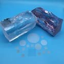
High-temperature...
High-temperature superconducting thin film substrates are specialized materials designed to support the deposition of high-temperature superconducting films, which exhibit zero electrical resistance at elevated temperatures. These substrates are essential for applications in advanced electronics, power transmission, and magnetic systems, where efficient energy transfer and minimal loss are critical.
Substrates for High-Temperature Superconducting Thin Films
These crystalline substrates are selected for high-temperature superconducting and oxide thin-film growth. Important factors include lattice and thermal compatibility, orientation, dimensions, thickness, miscut, surface roughness, flatness, polishing quality and termination.
Superconducting Film Substrate Selection
Specify the target film, substrate material, orientation, dimensions, thickness, miscut, polishing, roughness, flatness, termination, thermal process, packaging and quantity.
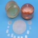
Magnetic and...
Heeger Materials offers magnetic and ferroelectric thin-film substrates known for their excellent crystal quality, structural stability, and strong compatibility with magnetic and ferroelectric films. These substrates are crucial in the development of memory devices, sensors, and actuators.
Magnetic and Ferroelectric Thin-Film Substrates
These substrates support magnetic, ferroelectric, multiferroic and functional oxide film growth. Selection depends on composition, dopant, orientation, lattice characteristics, miscut and polished surface quality.
Selection and Ordering Information
Specify target film, substrate composition and dopant, orientation, dimensions, thickness, miscut, polishing sides, roughness, flatness, termination and quantity.
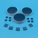
Semiconductor Thin...
Semiconductor thin film substrates are high-performance materials with excellent electrical properties, thermal stability, and structural integrity. These substrates provide a stable foundation for the fabrication of components such as integrated circuits, sensors, and power devices.
Semiconductor Thin-Film Substrates
Semiconductor substrates are selected for epitaxy, electronic and optoelectronic devices, detector research and process development. Key factors include composition, doping or conductivity, orientation, dimensions and surface preparation.
Selection and Ordering Information
Provide material, doping or conductivity, orientation, size, thickness, miscut, polishing, roughness, flatness, defect requirements, packaging and quantity.
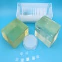
GaN Thin Film Substrates
GaN (Gallium Nitride) thin film substrates are cutting-edge materials designed to support the growth of high-performance GaN films, which are widely used in optoelectronics, power electronics, and RF devices. These substrates offer exceptional thermal conductivity, high breakdown voltage, and outstanding efficiency, making them ideal for applications in LEDs, power transistors, and wireless communication systems.
GaN Thin-Film Substrates
Compare substrate materials for GaN epitaxy, LEDs, power electronics, RF devices and nitride research. Selection factors include lattice compatibility, crystal orientation or polytype, dimensions, miscut, roughness and termination.
Selection and Ordering Information
Share the GaN growth method or structure, substrate material, orientation or polytype, size, thickness, miscut, polishing, roughness, termination and quantity.
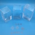
Halide Crystal Substrates
Halide crystal substrates are high-quality materials with excellent lattice matching and optical transparency, commonly used in the growth of optoelectronic and photonic devices. The common halide crystal substrates, such as sodium chloride (NaCl), potassium bromide (KBr), and cesium iodide (CsI), are ideal for applications in semiconductor research, lasers, and optical imaging systems.
Moisture-Sensitive Halide Crystal Substrate Selection
Halide crystal substrates support infrared and ultraviolet optics, spectroscopy, detector windows, thin-film research and thermoluminescent dosimetry. Moisture sensitivity and protective handling are important selection factors.
Selection and Ordering Information
Specify composition, orientation, dimensions, thickness, surface finish or cleavage, coating, moisture protection, packaging, quantity and intended optical or dosimetry use.
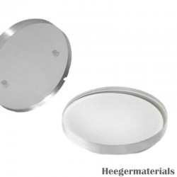
Potassium Bromide Crystal Substrate | KBr...
Potassium Bromide (KBr) Crystal Substrate is a highly transparent material with excellent infrared transmission, making it ideal for optical spectroscopy, thin-film deposition, and X-ray applications. Heeger Materials is a professional supplier and manufacturer of high-quality Potassium Bromide Crystal Substrate, offering customized solutions and...
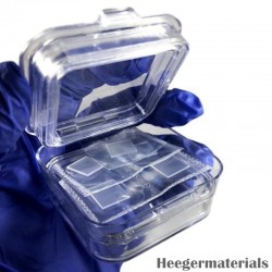
Lithium Fluoride Crystal Substrate | LiF...
Lithium Fluoride (LiF) Crystal Substrate is widely used in ultraviolet optics, including windows and prisms, due to its excellent UV transmission and high optical clarity. Heeger Materials is a professional supplier and manufacturer of high-quality Lithium Fluoride Crystal Substrate, offering customized solutions and competitive prices.
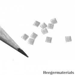
LiF:(Mg,Cu,P) Thermoluminescent Dosimeter...
LiF:(Mg,Cu,P) Thermoluminescent Dosimeter Chips are solid-state radiation detectors with high sensitivity and a low detection threshold, comparable to air or tissue. They are widely used in environmental, personal, and medical dosimetry, especially in low-background radiation fields.