

Substrates play a critical role in the performance of Radio Frequency (RF) and MicroLED technologies. These materials provide the necessary support for the active components of these devices and help manage thermal, electrical, and mechanical properties. As RF and MicroLED technologies evolve, the demand for advanced substrates with higher efficiency, thermal conductivity, and electrical performance grows. Two prominent materials that are considered for these applications are Sapphire and Aluminum Nitride (AlN).
Both materials have distinct properties that make them ideal for different applications. Sapphire is widely known for its use in optoelectronics, while AlN is emerging as a more promising option due to its excellent thermal conductivity and wide bandgap. This article will delve into a detailed comparison of Sapphire and AlN substrates for RF and MicroLED applications, highlighting their properties, advantages, and challenges.
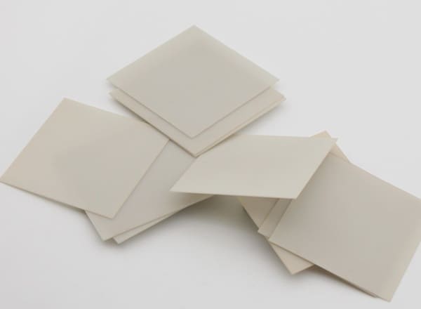
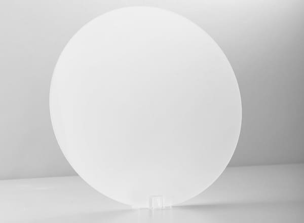
At Heeger Materials Inc., we specialize in high-quality aluminum nitride substrates and sapphire substrates with various specifications, ensuring optimal performance for industrial and scientific applications.
Properties of Sapphire Substrates
Sapphire, or aluminum oxide (Al₂O₃), is a single crystal with a hexagonal structure. It is one of the hardest materials known, making it extremely durable. Its structure provides excellent optical clarity, which is beneficial for certain optoelectronic devices, including MicroLEDs. Sapphire substrates are commercially available in various forms, including single crystals, wafers, and plates.
1. Physical Properties
Property | Value | Significance |
Crystal Structure | Hexagonal (α-Al₂O₃) | Anisotropic properties (vary with crystal orientation) |
Lattice Constants | a=4.758Å, c=12.991Å | Critical for epitaxial growth matching |
Density | 3.98 g/cm³ | Higher than silicon (2.33) but lower than GaN (6.15) |
Melting Point | 2053°C | Enables high-temperature processing |
Mohs Hardness | 9 (3rd hardest natural material) | Requires diamond tools for machining |
2. Thermal Properties
Parameter | Value | Comparison |
Thermal Conductivity | 35-46 W/m·K (⊥c-axis) | ~10× lower than AlN, but isotropic |
CTE (25-1000°C) | 7.5-8.5 ppm/K (⊥c-axis) | Better match to GaN (5.6) than silicon (4.1) |
Specific Heat Capacity | 0.76 J/g·K @25°C | Similar to quartz |
3. Electrical Properties
Characteristic | Value | Application Impact |
Bandgap | 8.8 eV (ultra-wide) | Excellent insulator (resistivity >10¹⁶ Ω·cm) |
Dielectric Constant | ε∥=9.4, ε⊥=11.6 (@1MHz) | Anisotropy affects RF device performance |
Breakdown Voltage | 15 MV/cm | Suitable for high-voltage devices |
4. Mechanical Properties
Property | Value | Manufacturing Considerations |
Young's Modulus | 345 GPa (c-axis) | Stiffer than silicon (170 GPa) |
Flexural Strength | 600-1000 MPa | Depends on the surface polish quality |
Fracture Toughness | 2.0 MPa·m¹/² | Requires careful handling to avoid chipping |
Knoop Hardness | 2000 kg/mm² | Only diamond/scCBN can be processed effectively |
5. Chemical Stability
Environment | Resistance Level | Notes |
Acids | Resists all except HF/H₃PO₄ | 10% HF etches at 100μm/hr @80°C |
Alkalis | Attacked by molten NaOH/KOH | Not suitable for strong alkali environments |
Plasma | Excellent | Common in semiconductor dry etching processes |
Oxidation | Fully stable | No oxide layer formation |
Looking for high-quality sapphire substrates? Explore Heeger Materials' selection.
Advantages of Sapphire for RF/MicroLED Applications
Sapphire remains unrivaled for cost-sensitive, high-performance RF and MicroLED applications below 40GHz and for pixel sizes <20μm.
Key Benefits:
- Mechanical Strength: Sapphire’s hardness and mechanical strength make it suitable for harsh environments, providing reliability in high-stress applications.
- Optical Clarity: Its transparency to UV light makes Sapphire ideal for applications requiring light emission or sensing, such as MicroLEDs.
- High Thermal Stability: Sapphire substrates can endure high operating temperatures, which is crucial for high-power RF components.
Its unique combination of RF purity, optical transparency, and thermal stability ensures continued dominance in:
- 5G/6G front-end modules
- AR/VR microdisplays
- Ultra-high-density LED arrays
Limitations of Using Sapphire
1. Thermal Management Constraints
✅Low Thermal Conductivity:
- 35-46 W/m·K (vs. 150 for Si, 490 for SiC)
- Limits power density to <5W/mm² for GaN RF devices
- Causes 15-20°C higher junction temps vs. SiC in 100W amplifiers
✅Thermal Resistance Challenges:
Device Type | Rθ(j-c) on Sapphire | Rθ(j-c) on SiC |
GaN HEMT (10mm) | 8 K/W | 2 K/W |
MicroLED Array | 12 K/W | N/A |
2. Electrical Limitations
Insulating Nature Creates Barriers:
- No vertical conductivity: Requires complex via technologies
- Backside grounding needs full wafer thinning (<100μm)
- RF losses increase exponentially above 40GHz
3. Manufacturing Challenges
Issue | Impact | Mitigation Cost |
Hard Machining | 50% higher dicing costs | +$0.10/mm cut length |
Wafer Size Limit | Max 8" diameter (vs. 12" Si) | 30% lower dies/wafer |
Epitaxial Defects | 10⁶ dislocations/cm² (GaN-on-sapphire) | +2 MOCVD cycles |
Properties of Aluminum Nitride Substrates
Aluminum Nitride (AlN) is a wide bandgap material with a hexagonal crystal structure, similar to Sapphire but with different characteristics that give it a distinct advantage in certain applications. AlN is known for its remarkable thermal conductivity, which makes it highly suitable for managing heat in high-power devices.
1. Physical Properties
Property | Value | Significance |
Crystal Structure | Wurtzite (hexagonal) | Similar to GaN, it enables lattice-matched epitaxial growth |
Lattice Constants | a=3.11Å, c=4.98Å | 2.4% mismatch with GaN (vs. 13% for sapphire) |
Density | 3.26 g/cm³ | Lighter than sapphire (3.98) and SiC (3.21) |
Melting Point | 2200°C | Suitable for high-temperature processing |
Hardness | 12 GPa (Vickers) | Requires diamond/CBN machining tools |
2. Thermal Properties
Parameter | Value | Advantage |
Thermal Conductivity | 170-220 W/m·K (polycrystalline) | 5-7× higher than Al₂O₃, approaches copper (400) |
CTE (25-300°C) | 4.5 ppm/K | Matches Si (4.1) and GaN (5.6), reducing thermal stress |
Specific Heat Capacity | 0.74 J/g·K | Efficient heat absorption |
3. Electrical Properties
Characteristic | Value | Application Impact |
Bandgap | 6.2 eV (direct) | Ultra-wide bandgap for high-power/high-frequency devices |
Resistivity | >10¹⁴ Ω·cm | Excellent insulator |
Dielectric Constant | 8.6 @1MHz | Low signal delay in RF applications |
Breakdown Field | 15 MV/cm | Withstands high voltages |
4. Mechanical Properties
Property | Value | Manufacturing Considerations |
Young's Modulus | 330 GPa | High stiffness for wafer handling |
Flexural Strength | 300-400 MPa | Comparable to sapphire |
Fracture Toughness | 3.2 MPa·m¹/² | Better than sapphire (2.0) but still brittle |
Poisson's Ratio | 0.23 | Important for stress modeling |
5. Chemical Stability
Environment | Resistance | Notes |
Acids | Resists most (except HF) | Stable in HCl/HNO₃ at RT |
Alkalis | Attacked by molten hydroxides | Not suitable for strong alkali environments |
Oxidation | Forms thin Al₂O₃ layer @>800°C | Self-passivating |
Moisture | Hydrolyzes slowly @>700°C | Requires protective coatings in steam |
Looking for high-quality aluminum nitride substrates? Explore Heeger Materials' selection.
Benefits of Aluminum Nitride for RF and MicroLED Technologies
Aluminum Nitride (AlN) substrates offer transformative advantages for next-generation RF and MicroLED applications, addressing critical limitations of traditional materials like silicon and sapphire.
- High Thermal Conductivity: AlN is one of the best materials for heat dissipation in high-power devices, ensuring long-lasting performance and stability.
- Electrical Insulation: AlN’s wide bandgap also provides excellent electrical insulation, making it suitable for high-frequency RF applications.
- Better Power Handling: AlN's ability to handle higher power densities is a crucial factor in RF and MicroLED applications where power efficiency is essential.
Challenges of Aluminum Nitride
Despite its exceptional thermal and electrical properties, Aluminum Nitride (AlN) faces several technical and economic hurdles that limit its widespread adoption.
- Cost and Fabrication Challenges: AlN is difficult to produce in large quantities due to its high manufacturing cost and complex crystal growth process.
- Brittleness: Similar to Sapphire, AlN is also a brittle material, making it susceptible to cracking under mechanical stress during handling and processing.
- Limited Scalability: The production techniques for AlN are still under development, and scaling them to large volumes remains a challenge.
1. Manufacturing Difficulties
A. High-Purity Synthesis
Oxygen Contamination:
- Even <100 ppm oxygen degrades thermal conductivity by 30–50% (from 220 W/m·K to ~150 W/m·K).
- Requires plasma-assisted nitridation or carbothermal reduction under ultra-clean conditions.
B. Sintering Challenges
Parameter | AlN Requirement | Typical Solution |
Temperature | >1800°C | Additives (Y₂O₃, CaO) lower to ~1600°C |
Pressure | 20–30 MPa | Hot pressing or spark plasma sintering |
Atmosphere | Nitrogen or vacuum | Prevents oxidation |
C. Wafer Scalability
- Max commercial wafer size: 6-inch (vs. 12-inch Si or 8-inch sapphire).
- Cracking risk increases beyond 150 μm thickness.
2. Material Limitations
A. Mechanical Brittleness
- Fracture toughness: 3.2 MPa·m¹/² (vs. 4.5 for SiC).
- Dicing yield loss: 20–30% due to chipping (requires laser scribing).
B. Electrical Constraints
No native p-type doping:
- Max hole concentration: ~10¹⁷ cm⁻³ (too low for bipolar devices).
- Limits applications in UV LEDs and high-power switches.
Dielectric loss increases at mmWave:
- tanδ rises from 0.0001 @10GHz to 0.005 @100GHz.
C. Thermal Boundary Resistance
Kapitza resistance at AlN/GaN interfaces:
- Adds 5–10 K·mm²/W thermal resistance.
- Requires atomic-layer engineered buffers (e.g., AlN nucleation layers).
Comparison of Sapphire and Aluminum Nitride for RF/MicroLED Applications
When choosing between sapphire and AlN substrates, a detailed comparison of their performance metrics is essential. The table below summarizes key properties relevant to RF and MicroLED applications:
Property | Sapphire | Aluminum Nitride |
Thermal Conductivity | 30–40 W/m·K | 170–200 W/m·K |
Dielectric Constant | ~9–11 | ~8.5 |
Dielectric Loss | Low | Low |
Bandgap | 9.9 eV | 6.2 eV |
Optical Transparency | Transparent (UV to IR) | Opaque |
Lattice Constant (a-axis) | 4.758 Å | 3.112 Å |
Hardness (Mohs) | 9 | 7 |
✅Thermal Conductivity: AlN’s superior thermal conductivity makes it the preferred choice for high-power RF devices, where heat dissipation is critical to prevent performance degradation. Sapphire, with its lower thermal conductivity, may struggle in applications with high thermal loads, requiring additional cooling mechanisms.
✅Electrical Performance: Both substrates offer low dielectric loss, essential for minimizing signal attenuation in RF applications. Sapphire’s slightly higher dielectric constant provides a marginal advantage in certain RF designs, but AlN’s performance is comparable and often sufficient.
✅Mechanical and Optical Properties: Sapphire’s hardness and transparency make it ideal for MicroLED displays, where durability and light extraction are key. AlN’s opacity limits its use in optical applications, but its mechanical strength is adequate for RF devices.
✅Lattice and Thermal Expansion Matching: AlN’s closer lattice match with GaN (lattice mismatch ~1%) compared to sapphire (~13%) reduces defects during epitaxy, improving device reliability. Additionally, AlN’s thermal expansion coefficient (4.2 × 10⁻⁶/K) is closer to GaN (5.6 × 10⁻⁶/K) than sapphire (7.5 × 10⁻⁶/K), minimizing stress during thermal cycling.
Explore our optimized aluminum nitride substrates and sapphire substrates.
How to Choose the Right Substrate for Specific Applications?
Selecting the optimal substrate (Sapphire vs. Aluminum Nitride, AlN) depends on performance requirements, cost constraints, and application-specific needs.
1. Key Selection Criteria
Parameter | Sapphire (Al₂O₃) | Aluminum Nitride (AlN) | Dominant Factor |
Thermal Conductivity | 35–46 W/m·K | 170–220 W/m·K | High-power devices → AlN |
Cost (6-inch wafer) | $200–$400 | $800–$1200 | Budget-sensitive → Sapphire |
RF Loss (tanδ @10GHz) | 0.0004 | 0.0001 | mmWave (>30GHz) → AlN |
Lattice Match to GaN | 13% mismatch | 2.4% mismatch | Low-defect epitaxy → AlN |
Optical Transparency | Transparent (UV–IR) | Opaque | MicroLED light extraction → Sapphire |
Mechanical Strength | Hard (Mohs 9) | Brittle (3.2 MPa·m¹/²) | Durability → Sapphire |
2. Selection Guide for Key Applications
Application | Recommended Substrate | Key Advantages | Best For |
RF Applications | Aluminum Nitride (AlN) | - Superior thermal conductivity (170–220 W/m·K) | 5G mmWave, satellite comms, radar systems |
MicroLED Displays | Sapphire (Al₂O₃) | - Optical transparency (85% UV–IR) | Consumer displays (TVs, tablets), AR/VR (pixels >5μm) |
High-Power Electronics | Aluminum Nitride (AlN) | - Exceptional heat dissipation (5–7× better than sapphire) | EV inverters, industrial motor drives, aerospace power systems |
Cost-Sensitive Applications | Sapphire (Al₂O₃) | - Lower cost ($200–$400 per 6-inch wafer vs. AlN’s $800–$1200) | IoT devices, consumer 5G, LED lighting |
Request a custom quote for high-quality aluminum nitride substrates and sapphire substrates.
At Heeger Materials Inc., we supply optimized-grade ceramic products that comply with ASTM and ISO standards, ensuring outstanding quality and reliability.
Both Sapphire and Aluminum Nitride offer unique advantages depending on the application. Sapphire is widely used in optoelectronics and low-power applications, offering great durability and optical properties. AlN, on the other hand, stands out for its high thermal conductivity and ability to handle high-power densities, making it ideal for RF and high-power applications.
In conclusion, the choice between Sapphire and AlN substrates comes down to the specific needs of the application, including factors such as power handling, thermal management, cost, and scalability. With advancements in materials science and manufacturing techniques, both substrates are likely to play crucial roles in the future of RF and MicroLED technologies.
For top-quality ceramic materials, Heeger Materials provides tailored solutions for various applications.
Looking for premium aluminum nitride substrates and sapphire substrates? Contact us today!