Viewed products
-

Silicon Dioxide...
Silicon Dioxide (SiO2) Crystal is a...
Photoelectric Crystals
- Products
- Deposition Materials
- Refractory Metals
- Rare Earth Materials
- Powder
- Technical Ceramics
- Lanthanum Hexaboride (LaB6) Materials
- Pyrolytic Boron Nitride (PBN) Products
- Boron Nitride (BN) Products
- Alumina Ceramics (Al2O3)
- Aluminum Nitride (AlN) Products
- Silicon Nitride (Si3N4) Ceramics
- Silicon Carbide (SiC) Ceramics
- Graphite Products
- Zirconia Ceramic
- MAX Phase Ceramic Materials
- Boron Carbide Ceramics (B4C)
- Magnesium Oxide Ceramics (MgO)
- Quartz Ceramics
- Macor Machinable Glass Ceramic
- Beryllium Oxide (BeO) Ceramics
- Piezoelectric Ceramics
- High Purity Materials
- Precious Metals
- Chemicals
- Crystals & Substrates
- Applications
- Other
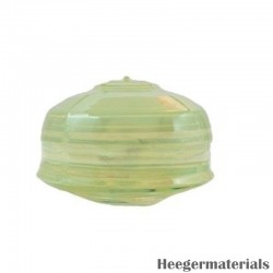
 View larger
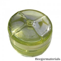
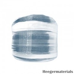
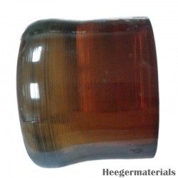
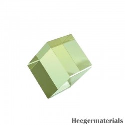
Silicon Dioxide Crystal | SiO2 Crystal
HM2799
New product
Silicon Dioxide (SiO2) Crystal is a highly stable and transparent material known for its exceptional optical properties. With low thermal expansion and high hardness, it's widely used in optical and electronic applications, including lenses, windows, and sensor components. Heeger Materials (HM) provides high-quality SiO2 crystals for reliable performance in advanced technology systems.
Please contact us if you need customized services. We will contact you with the price and availability in 24 hours.
Data sheet
| Density | 2.684g/cm3 |
| Melting Piont | 1610℃ |
| Molecular Formula | SiO2 |
More info

Silicon Dioxide Crystal | SiO2 Crystal Selection Notes
Silicon Dioxide Crystal | SiO2 Crystal belongs to the photoelectric crystal range and is selected for controlled crystal composition, orientation or cut, dimensions, optical surface quality and electrode or coating requirements. It is commonly used in electro-optic modulators, frequency conversion, piezoelectric devices, optical sensing, photorefractive research and laser systems. When requesting a quote, confirm crystal composition, orientation or cut, dimensions, domain or poling requirement, optical surface quality, electrodes or coating, target wavelength, documentation and quantity.
Related Materials and Product Forms
For material comparison or adjacent product forms, browse photoelectric crystals, semiconductor crystals and crystals and substrates.
FAQ
What cut and optical details are needed for Silicon Dioxide Crystal | SiO2 Crystal? Please provide crystal cut or orientation, dimensions, poling or domain requirement, surface quality, electrode or coating needs, wavelength, documentation, quantity and intended electro-optic or piezoelectric application.
Silicon Dioxide Crystal Properties
Growth Method | Hydrothermal Method |
Crystal Structure | Hexagonal |
Lattice Constants | a = 4.914 Å, c = 5.405 Å |
Density | 2.684 g/cm³ |
Hardness | 7 (Mohs) |
Specific Heat Capacity | 0.18 cal/gm |
Melting Point | 1610℃ (Phase - transition Point: 573.1℃) |
Thermal Conductivity | 0.0033 cal/cm℃ |
Pyroelectric Constant | 1200 uv/℃ (300℃) |
Refractive Index | 1.544 |
Thermal Expansion Coefficients | α11: 13.71×10⁻⁶ /℃, α33: 7.48×10⁻⁶ /℃ |
Q - value | 1.8×10⁶ min |
Sound velocity, surface acoustic wave level | 3160 (m/sec) |
Frequency Constant | 1661 (kHz/mm) |
Piezoelectric Coupling | K²(%): BAW: 0.65, SAW: 0.14 |
Packaging Material | IEC Grade II |
Silicon Dioxide Crystal Specifications
Orientation | Y, X, or Z - cut, rotated at any value within 30º-42.75º ± 5 minutes of arc. Main orientation flat: Direction determined according to customer requirements ± 30 minutes of arc. Secondary orientation flat: Direction determined according to customer requirements. Seed crystal: Located at the center, with width < 5mm and height > 66mm. |
Polished Surfaces | Epitaxial polishing: Single-side or double-side polished, Ra < 10Å. Working area: Substrate diameter - 3mm. Bow: Φ3″ < 20um, Φ4″ < 30um. No edge chipping in the working area. At the edge, the chipping width is < 0.5mm. Pits and scratches: < 3 per piece, < 20 per 100 pieces. |
Standard Thickness | 0.5mm ± 0.05mm, TTV < 5um |
Standard Diameter | Φ2″ (50.8mm), Φ3″ (76.2mm), Φ4″ (100mm) ± 0.2mm. Main orientation flat: 22 ± 1.5mm (for Φ3″), 32 ± 3.0mm (for Φ4″). Secondary orientation flat: 10mm ± 1.5mm. |
Silicon Dioxide Crystal Applications
- Nonlinear optical components: Employed in creating optical parametric oscillation (OPO) and second-harmonic generation (SHG) systems for sophisticated laser technologies.
- Optical Modulators: Employed in electro-optical modulation systems for communication and signal processing applications.
- Infrared Optics: Employed in infrared optical systems because of its excellent transmittance in the infrared range at mid-to-long wavelengths.
- Piezoelectric Devices: Utilized in manufacturing piezoelectric devices for sensors and actuators.
- Laser Sources and Detectors: Crucial for the progress of high-performance laser sources and detectors used in scientific and industrial applications.
Silicon Dioxide Crystal Packing And Shipping
Silicon Dioxide (SiO2) Crystal will be securely packaged in sturdy containers with cushioning materials to prevent movement or damage during shipping. This careful packaging ensures that the product arrives in perfect condition, maintaining its high-quality standards throughout the delivery process.

Where to Buy Silicon Dioxide Crystal in Bulk?
Heeger Materials Inc., a professional supplier and manufacturer of high-quality Photoelectric Crystals including Silicon Dioxide (SiO2) Crystal, leverages extensive expertise in supply and export to offer competitive prices. We provide customized solutions to meet specific requirements, ensuring exceptional quality and customer satisfaction.
Heeger Materials Inc. was established in 2016 in Colorado, USA. We specialize in premium-grade metals, alloys, ceramics, powders, and other materials catering to research, development, and large-scale industrial production in scientific and industrial sectors.
Inquiry to Heeger Materials
Items marked with an asterisk (*) are required.
Heeger Materials respects your privacy, and we will NOT sell or provide your personal data to other third parties, or allow them to use your personal data for their own purposes. However, we would like to send you information from time to time by mail or email about our products and special offers in addition to the interest categories you've selected above. Read our Privacy Policy