

Semiconductor technology has been evolving with each generation, utilizing different materials that offer unique characteristics and applications. The first generation employed traditional materials such as Silicon (Si) and Germanium (Ge). The second generation introduced compound semiconductors like Gallium Arsenide (GaAs), Indium Phosphide (InP), and Cadmium Telluride (CdTe). The third generation utilizes new materials like Gallium Nitride (GaN), Silicon Carbide (SiC), and Zinc Oxide (ZnO). Currently, SiC is the most mature wide bandgap power semiconductor material, followed by GaN. Diamond, Aluminum Nitride (AlN), and Gallium Oxide (Ga2O3) are also prominent in international research.
This blog post is about a new semiconductor, BAs. BAs is an ideal semiconductor material with excellent thermal conductivity and desirable properties. Unlike expensive and challenging materials like diamond and graphene, BAs offer a practical solution for electronic devices.
BAs has a thermal conductivity almost ten times higher than silicon, making it ideal for heat dissipation. It also has an excellent bandgap, making it a promising semiconductor material.
Properties | Si | GaAs | BAs |
Thermal conductivity k (Wm-1K-1) | 140 | 45 | 1300 |
Electron mobility me (cm2V-1s-1) | 1400 | 8500 | 1400 |
Hole mobility mh (cm2V-1s-1) | 450 | 400 | 1600 |
Band gap (eV) | 1.1 | 1.4 | 2.0 |
Coe.of thermal expansion (x10-6K-1) | 2.6 | 6.9 | 4.2 |
BAs has high electron and hole mobility, making it an ideal semiconductor material. It has low resistance to charge movement and superior thermal conductivity compared to silicon. GaAs could potentially revolutionize heat dissipation and electronic device manufacturing. However, SiC is still preferred for power electronics due to its higher thermal conductivity, despite its lower electron mobility.
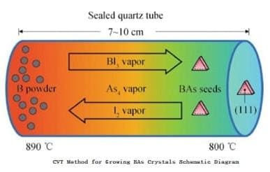
The growth of BAs crystals faces challenges due to factors such as the high melting point of boron, the toxicity of arsenic, the chemical stability of boron, and the decomposition of BAs at high temperatures. These challenges make the melt method less suitable for BAs crystal growth. However, the chemical vapor transport (CVT) method has emerged as a solution, allowing precise temperature control and addressing the challenges effectively.
BAs is a promising semiconductor material with high thermal conductivity and excellent properties. Despite challenges in crystal growth, methods like CVT offer new possibilities. As technology advances, BAs may play a significant role in shaping the future of electronic devices.
Heeger Materials is a reputable supplier offering top-notch Rear Earth Materials and Semiconductor Materials products at competitive prices, which are widely used in semiconductor industries and science fields. If you're interested, feel free to reach out to us at [email protected] for a quote, and we guarantee a response within 24 hours.