

Viewed products
-

Gold/Chromium/Silicon...
Gold/Chromium/Silicon (Au/Cr/Si)...
Epitaxial Thin Film
- Products
- Deposition Materials
- Refractory Metals
- Rare Earth Materials
- Powder
- Technical Ceramics
- Lanthanum Hexaboride (LaB6) Materials
- Pyrolytic Boron Nitride (PBN) Products
- Boron Nitride (BN) Products
- Alumina Ceramics (Al2O3)
- Aluminum Nitride (AlN) Products
- Silicon Nitride (Si3N4) Ceramics
- Silicon Carbide (SiC) Ceramics
- Graphite Products
- Zirconia Ceramic
- MAX Phase Ceramic Materials
- Boron Carbide Ceramics (B4C)
- Magnesium Oxide Ceramics (MgO)
- Quartz Ceramics
- Macor Machinable Glass Ceramic
- Beryllium Oxide (BeO) Ceramics
- Piezoelectric Ceramics
- High Purity Materials
- Precious Metals
- Chemicals
- Crystals & Substrates
- Applications
- Other
 View larger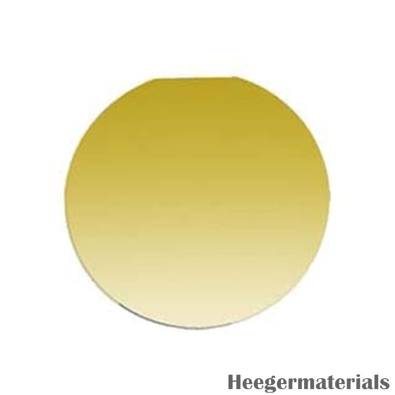
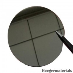
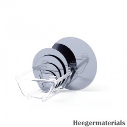
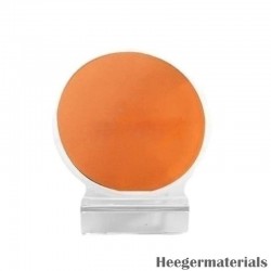
Gold/Chromium/Silicon Epitaxial Wafer | Au/Cr/Si Wafer
HM2936
New product
Gold/Chromium/Silicon (Au/Cr/Si) Epitaxial Wafer features a gold layer with a chromium adhesion layer on a silicon substrate, making it ideal for microelectronics, MEMS, and semiconductor applications. Heeger Materials is a professional supplier and manufacturer of high-quality Au/Cr/Si Wafers, offering customized solutions and competitive prices.
Please contact us if you need customized services. We will contact you with the price and availability in 24 hours.
Data sheet
| Materials | Au/Cr/Si Wafer |
More info
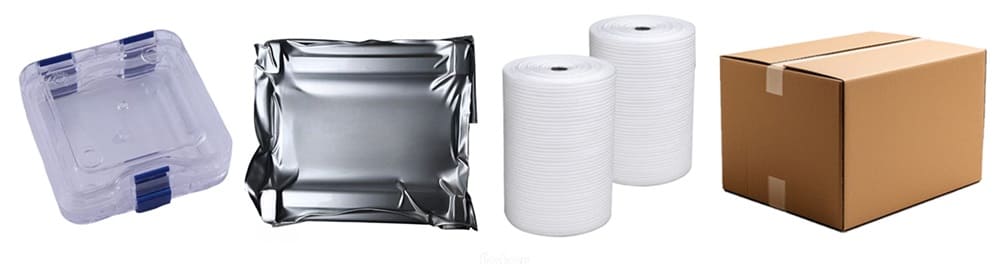
Gold/Chromium/Silicon (Au/Cr/Si) Epitaxial Wafer will be securely packaged in sturdy containers with cushioning materials to prevent movement or damage during shipping. This careful packaging ensures that the product arrives in perfect condition, maintaining its high-quality standards throughout the delivery process.
Where to Buy Gold/Chromium/Silicon Epitaxial Wafer in Bulk?
Heeger Materials Inc., a professional supplier and manufacturer of high-quality Epitaxial Thin Film products including Gold/Chromium/Silicon (Au/Cr/Si) Epitaxial Wafer, leverages extensive expertise in supply and export to offer competitive prices. We provide customized solutions to meet specific requirements, ensuring exceptional quality and customer satisfaction.
Heeger Materials Inc. was established in 2016 in Colorado, USA. We specialize in premium-grade metals, alloys, ceramics, powders, and other materials catering to research, development, and large-scale industrial production in scientific and industrial sectors.
Inquiry to Heeger Materials
Items marked with an asterisk (*) are required.
Heeger Materials respects your privacy, and we will NOT sell or provide your personal data to other third parties, or allow them to use your personal data for their own purposes. However, we would like to send you information from time to time by mail or email about our products and special offers in addition to the interest categories you've selected above. Read our Privacy Policy