

Wafers & Substrates
- Products
- Deposition Materials
- Refractory Metals
- Rare Earth Materials
- Powder
- Technical Ceramics
- Lanthanum Hexaboride (LaB6) Materials
- Pyrolytic Boron Nitride (PBN) Products
- Boron Nitride (BN) Products
- Alumina Ceramics (Al2O3)
- Aluminum Nitride (AlN) Products
- Silicon Nitride (Si3N4) Ceramics
- Silicon Carbide (SiC) Ceramics
- Graphite Products
- Zirconia Ceramic
- MAX Phase Ceramic Materials
- Boron Carbide Ceramics (B4C)
- Magnesium Oxide Ceramics (MgO)
- Quartz Ceramics
- Macor Machinable Glass Ceramic
- Beryllium Oxide (BeO) Ceramics
- Piezoelectric Ceramics
- High Purity Materials
- Precious Metals
- Chemicals
- Crystals & Substrates
- Applications
- Other
Our wafers and substrates include Silicon, GaAs, GaN, and Sapphire materials, ideal for electronics, optoelectronics, and solar applications. Their excellent crystal quality and precise thickness control ensure superior performance in semiconductor devices, integrated circuits, and solar cells.
Our wafers and substrates include Silicon, GaAs, GaN, and Sapphire materials, ideal for electronics, optoelectronics, and solar applications. Their excellent crystal quality and precise thickness control ensure superior performance in semiconductor devices, integrated circuits, and solar cells.
Wafers & Substrates There are 79 products.
Subcategories
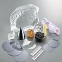
Single Crystal Substrates
Single crystal substrates are highly pure materials with a uniform atomic structure, providing an ideal foundation for the growth of high-quality thin films and semiconductor devices. These substrates are essential in industries such as electronics, optoelectronics, and photonics, where precise material properties and defect-free surfaces are critical. Common materials for single crystal substrates include silicon, sapphire, and gallium nitride, offering superior performance in applications like LED production, solar cells, and integrated circuits.
Single Crystal Substrates for Epitaxial Thin Films
Single crystal substrates support epitaxial film growth, oxide electronics, photonics, surface science and materials development. Selection depends on substrate composition, orientation, dimensions, thickness, miscut, polishing sides, roughness, flatness, termination and packaging.
Substrate Ordering Information
Provide material, orientation, size, thickness, miscut, one-side or double-side polishing, roughness, flatness, surface termination or coating, quantity and intended film or device process.
Thin Film Substrates
Thin film substrates are materials designed to support the deposition of thin films, providing a stable and reliable foundation for the fabrication of advanced electronic, optical, and energy devices. These substrates are commonly used in semiconductor manufacturing, solar cells, displays, and sensors, where precise control over surface properties and material compatibility is essential.
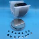
Epitaxial Thin Film
Epitaxial thin films are precisely grown layers of material that are deposited on a substrate with a highly ordered crystal structure, ensuring that the thin film's properties align with the underlying substrate. These films offer exceptional electrical, optical, and mechanical properties, and are critical in making advanced semiconductor devices, such as LEDs, solar cells, and integrated circuits. Epitaxial thin films
Epitaxial Thin Films and Wafers
Epitaxial thin-film products are supplied for semiconductor devices, optoelectronics, heterostructures and materials research. Compare substrate, layer sequence, composition, thickness, doping, orientation and surface quality.
Selection and Ordering Information
Provide the substrate, epitaxial layer stack, composition, layer thickness, doping or conductivity, orientation, wafer size, surface finish, characterization and quantity.
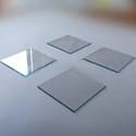
Conductive Glass...
Conductive Glass Substrates are specially designed materials that combine the transparency of glass with excellent electrical conductivity, making them ideal for use in electronic and optoelectronic devices.
Glass and Conductive Glass Substrates
This category includes quartz, optical glass and transparent conductive coated glass for optics, displays, sensors, thin films and electronic devices. Compare glass type, optical quality, coating, transmission and sheet resistance.
Selection and Ordering Information
Provide glass type, size, thickness, surface quality, flatness, coating and sheet resistance when applicable, transmission range, edge finish, packaging and quantity.
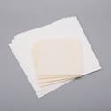
Ceramic Substrates
Ceramic substrates offer excellent thermal conductivity, electrical insulation, and mechanical strength. They are particularly essential in high-temperature environments and are widely used in power electronics, automotive components, and LED technology.
Ceramic Substrates for Electronic Assemblies
Ceramic substrates combine electrical insulation, thermal management and dimensional stability for power electronics, circuits, sensors and semiconductor packaging. Metallized options require controlled patterns and adhesion.
Selection and Ordering Information
Specify ceramic grade, dimensions, thickness, flatness, surface finish, metallization material and pattern, plating or adhesion requirements, drawing, packaging and quantity.
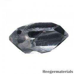
Quartz Crystal Materials | SiO2 Crystal
Quartz (SiO2) Crystal Materials are high-purity, single-crystal quartz grown under controlled hydrothermal conditions. With exceptional piezoelectric properties, they are widely used in frequency control devices, optical applications, and advanced scientific research
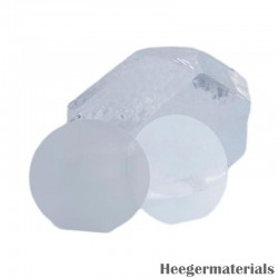
Quartz Single Crystal Wafer | SiO2 Wafer
Quartz (SiO2) Single Crystal Wafer features high purity, precise orientation, and excellent piezoelectric properties for resonators, oscillators, and optical applications. Heeger Materials is a professional supplier and manufacturer of high-quality Quartz Single Crystal Wafers, offering customized solutions and competitive prices.
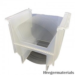
Corning 7980 Glass Substrate
orning 7980 Glass Substrate is a high-purity synthetic fused silica with excellent optical and thermal properties, featuring over 90% transmittance from 200 nm to 2500 nm. It offers low thermal expansion, strong durability, and is available in various grades for photonics and semiconductor applications.
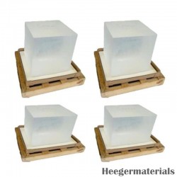
Ohara SK1300 Glass Substrate
Ohara SK1300 Glass Substrate is a high-purity optical glass with low hydroxyl (OH) content, offering excellent transmission in UV and visible light. It features strong mechanical properties, thermal resistance, and chemical durability, making it suitable for semiconductor and display applications.
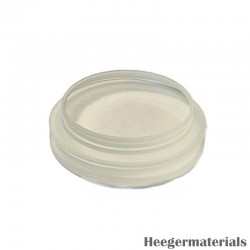
Schott Float/Borosilicate Glass Substrate
Schott Float/Borosilicate Glass Substrate is a high-quality glass known for its excellent optical clarity, low thermal expansion, and chemical resistance. It offers high transmission across the spectrum and withstands temperatures up to 450°C, making it suitable for optical, semiconductor, and microelectronics applications.
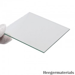
Aluminum-Doped Zinc Oxide Glass | AZO...
Aluminum-Doped Zinc Oxide (AZO) Glass is a transparent conductive oxide (TCO) substrate with excellent optical and electrical properties. It offers high transmittance in the visible spectrum and low electrical resistivity, making it ideal for optoelectronic applications.
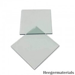
Indium Tin Oxide Conductive Glass | ITO...
Indium Tin Oxide (ITO) Conductive Glass is a transparent conductive substrate widely used in optoelectronic applications. It offers high optical transparency, excellent electrical conductivity, and uniform coating, making it ideal for displays, touch panels, and solar cells.
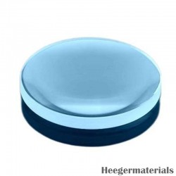
K9 Optical Glass | Borosilicate Optical Glass
K9 Optical Glass, also called Borosilicate Optical Glass, is a high-quality borosilicate optical glass known for its excellent transparency, low dispersion, and high refractive index. It is widely used in precision optics, laser systems, and optical instruments. HM is a professional supplier and manufacturer of high-quality K9 Optical Glass, offering...
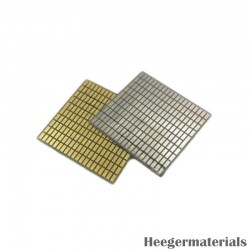
Metalized Aluminum Nitride Substrate | AlN...
Metalized Aluminum Nitride (AlN) Substrate combines high thermal conductivity, electrical insulation and metallized surfaces for power electronics, RF devices, LED modules and semiconductor packaging. Custom size, thickness and metallization options are available.
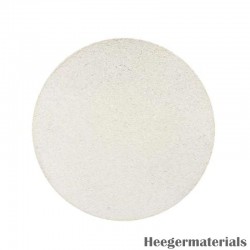
Yttrium-Stabilized Zirconia Sputtering...
Yttrium-Stabilized Zirconia (YSZ) Sputtering Target is a durable ceramic material with high ionic conductivity, thermal stability, and chemical resistance, widely used in fuel cells, sensors, and protective coatings. Heeger Materials is a professional supplier and manufacturer of high-quality YSZ sputtering targets, offering customized solutions and...
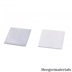
Aluminum Nitride On Diamond
Aluminum Nitride On Diamond offers superior thermal conductivity, high breakdown strength, and excellent stability, making it ideal for advanced electronic and optoelectronic applications. Heeger Materials is a professional supplier and manufacturer of high-quality AlN On Diamond, offering customized solutions and competitive prices.
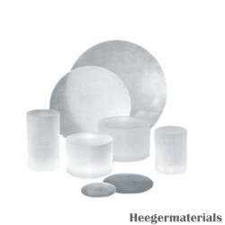
Sapphire Substrate
Sapphire Substrate offers excellent hardness, thermal stability, and optical clarity, ideal for LED, GaN, and infrared applications. Heeger Materials is a professional supplier and manufacturer of high-quality Sapphire Substrate, offering customized solutions and competitive prices.