Viewed products
-

Boron (B) Sputtering...
Boron Sputtering Target can be used...
Sputtering Targets
- Products
- Deposition Materials
- Refractory Metals
- Rare Earth Materials
- Powder
- Technical Ceramics
- Lanthanum Hexaboride (LaB6) Materials
- Pyrolytic Boron Nitride (PBN) Products
- Boron Nitride (BN) Products
- Alumina Ceramics (Al2O3)
- Aluminum Nitride (AlN) Products
- Silicon NItride (Si3N4) Ceramics
- Silicon Carbide (SiC) Ceramics
- Graphite Products
- Zirconia Ceramic
- MAX Phase Ceramic Materials
- Boron Carbide Ceramics (B4C)
- Magnesium Oxide Ceramics (MgO)
- Quartz Ceramics
- Macor Machinable Glass Ceramic
- Beryllium Oxide (BeO) Ceramics
- Piezoelectric Ceramics
- High Purity Materials
- Precious Metals
- Chemicals
- Crystals & Substrates
- Applications
- Other
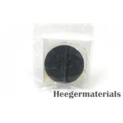
Boron (B) Sputtering Target
New product
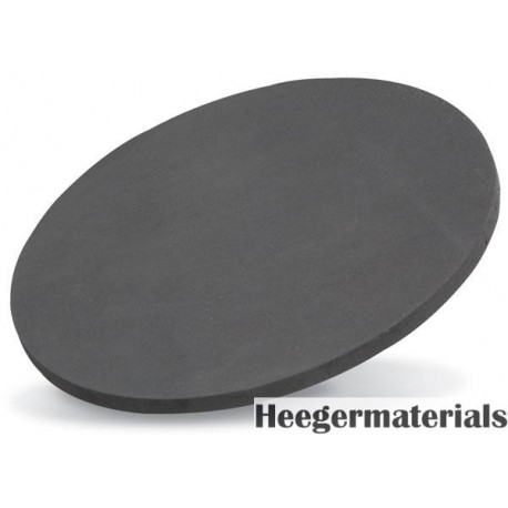
Boron Sputtering Target can be used in semiconductors, chemical vapor deposition (CVD), physical vapor deposition (PVD) display, and optical applications. We are a supplier of high-quality Boron Sputtering Target at competitive prices.
Please contact us if you need customized services. We will contact you with the price and availability in 24 hours.
Data sheet
| Shape | Disc/Rectangular/Tube |
| Bonding | Unbonding/Bonding |
| Symbol | B |
| Purity | 99.5% |
More info
Boron (B) Sputtering Targets are frequently utilized in thin-film deposition techniques, where boron is applied to substrates to form high-quality, long-lasting films. These targets are vital for a range of applications, such as semiconductor production, optical coatings, and durable coatings. Boron films offer outstanding characteristics, including remarkable wear resistance, corrosion resistance, and good electrical conductivity. In the semiconductor sector, boron is frequently utilized for doping during the production of electronic devices. Moreover, boron coatings are utilized in cutting tools, aerospace parts, and protective layers because of their toughness and longevity. Boron sputtering targets can be found in both pure and alloyed varieties for custom applications.HM provides high-quality Boron Sputtering Target for research and industry purposes at competitive prices. We can provide Boron Sputtering Target with different purity, size, and density according to your requirements.
- High purity and density
- Low particle
- Uniform film thickness distribution
- High efficiency in the use
Boron (B) Sputtering Target Specifications
Material Type | Boron |
Symbol | B |
Atomic Weight | 10.811 |
Atomic Number | 5 |
Color/Appearance | Black, Semi-metallic |
Thermal Conductivity | 27 W/m.K |
Melting Point (°C) | 2,079 |
Coefficient of Thermal Expansion | 6 x 10⁻⁶/K |
Theoretical Density (g/cc) | 2.34 |
Z Ratio | 0.389 |
Sputter | RF |
Max Power Density (Watts/Square Inch) | 20* |
Type of Bond | Indium |
Boron (B) Sputtering Target Dimensions
Circular Sputtering Targets | Diameter | 1.0” 2.0” 3.0” 4.0” 5.0” 6.0” up to 21” |
Rectangular Sputtering Targets | Width x Length | 5” x 12” 5” x 15” 5” x 20” 5” x 22” 6” x 20” |
Thickness | 0.125”, 0.25” | |
Sputtering Targets Requirements
General requirements such as size, flatness, purity, impurity content, density, N/O/C/S, grain size, and defect control. Special requirements include surface roughness, resistance value, grain size uniformity, composition and tissue uniformity, magnetic conductivity, ultra-high density, ultra-fine grains, etc.
Boron (B) Sputtering Target Applications
- Semiconductor Production: Boron sputtering targets are utilized to dope semiconductors, incorporating boron to alter the electrical characteristics of silicon wafers.
- Thin Film Coatings: Boron sputtering targets are used to produce thin films for electronics, optics, and solar cells. These films enhance hardness, abrasion resistance, and optical characteristics.
- Magnetic Materials: Boron sputtering targets serve to create magnetic materials such as hard drives and sensors. Boron enhances their magnetic characteristics.
- Solar Cells: Boron enhances the efficiency of thin-film solar cells. Boron sputtering targets are utilized to produce boron-doped films that enhance the efficiency of solar energy conversion.
- Plasma Display Panels (PDPs): Boron sputtering targets are utilized in plasma display panels to enhance display quality and energy efficiency.
Boron (B) Sputtering Target Delivery and Packaging
The Lead time of the Boron Sputtering Target is 2-5 weeks. It will be packaged in a vacuum-sealed plastic bag with a moisture barrier. The MSDS and COA will be packed with the product.
Customized Sputtering Targets
Heeger Materials specializes in producing custom compositions for commercial and research applications and for new proprietary technologies. Other magnetron sputtering targets, evaporation sources, and deposition materials are listed by material throughout the website.
Inquiry to Heeger Materials
Items marked with an asterisk (*) are required.
Heeger Materials respects your privacy, and we will NOT sell or provide your personal data to other third parties, or allow them to use your personal data for their own purposes. However, we would like to send you information from time to time by mail or email about our products and special offers in addition to the interest categories you've selected above. Read our Privacy Policy


