



Viewed products
-

Selenide Targets
Selenide Target is often used to coat...
Semiconductor Materials
- Products
- Deposition Materials
- Refractory Metals
- Rare Earth Materials
- Powder
- Technical Ceramics
- Lanthanum Hexaboride (LaB6) Materials
- Pyrolytic Boron Nitride (PBN) Products
- Boron Nitride (BN) Products
- Alumina Ceramics (Al2O3)
- Aluminum Nitride (AlN) Products
- Silicon Nitride (Si3N4) Ceramics
- Silicon Carbide (SiC) Ceramics
- Graphite Products
- Zirconia Ceramic
- MAX Phase Ceramic Materials
- Boron Carbide Ceramics (B4C)
- Magnesium Oxide Ceramics (MgO)
- Quartz Ceramics
- Macor Machinable Glass Ceramic
- Beryllium Oxide (BeO) Ceramics
- Piezoelectric Ceramics
- High Purity Materials
- Precious Metals
- Chemicals
- Crystals & Substrates
- Applications
- Other
 View larger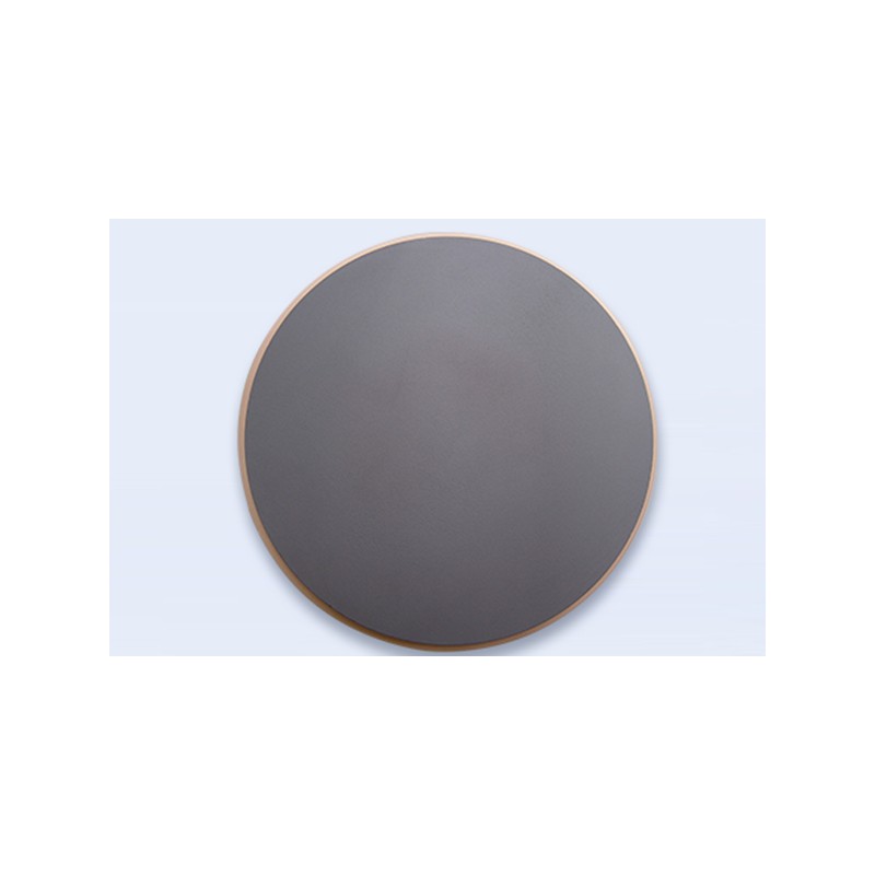
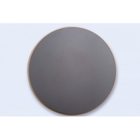
Selenide Targets
HM1344
New product
Selenide Target is often used to coat thin films of solar cells and the semiconductor industry. Heeger Materials specializes in high-quality Selenide for use in semiconductor, chemical vapor deposition (CVD), and physical vapor deposition (PVD) display and optical applications.
Please contact us if you need customized services. We will contact you with the price and availability in 24 hours.
Data sheet
| Molecular Formula | Cu2Se, Bi2Se3, In2Se3, Ga2Se3 |
| Purity | 99.99% - 99.999% |
More info
Selenide Targets are materials used for thin film deposition, composed of selenium and other metallic elements. HM provides high-quality Selenide Target at a competitive price, which can be used in Scientific research or industrial production. Different sizes and shapes can be tailored according to specific requirements.

- Formula: Cu2Se, Bi2Se3, In2Se3, (In,Ga)2Se3
- CAS No.: 7446-08-4
- EINECS No.: 231-957-4
- Purity: 99.99% min
- Size: 50.8mm - 300mm
- Melting Point: 217°C
- Boiling Point: 684.9°C
Selenide Targets Selection Notes
Selenide Targets belongs to the semiconductor compound material range and is selected for controlled material quality, application-specific specifications and reliable supply for research or production use. It is commonly used in compound semiconductor research, thin-film deposition, thermoelectric materials, infrared materials, phase-change materials and optoelectronic development. When requesting a quote, confirm compound composition, purity, form, particle size when powder, stoichiometry, impurity limits, packaging and quantity.
Related Materials and Product Forms
For material comparison or adjacent product forms, browse all products, deposition materials, technical ceramics and Semiconductor Materials.
FAQ
What semiconductor compound details help with quoting? Please provide compound composition, purity, form, particle size if applicable, stoichiometry or impurity limits, packaging and intended semiconductor or thin-film use.
Selenide Targets Advantages
- The source of the material is stable
- High purity, up to 99.999%
- High target density
- Stable quality
- Smooth and flat surface
Selenide Targets Applications
- Coating thin film of solar cell and semiconductor industry
- Used for magnetron sputtering of optoelectronic materials
- Evaporation coating
- Doping of semiconductor materials
Selenide Targets Packing
Selenide Targets should be securely sealed in a plastic bag and placed outside with either a carton or a bucket for storage and shipping.
Inquiry to Heeger Materials
Items marked with an asterisk (*) are required.
Heeger Materials respects your privacy, and we will NOT sell or provide your personal data to other third parties, or allow them to use your personal data for their own purposes. However, we would like to send you information from time to time by mail or email about our products and special offers in addition to the interest categories you've selected above. Read our Privacy Policy
30 other products in the same category:
-
Copper (I)...
-
Germanium...
-
Copper...
-
Copper...
-
Zinc...
-
Tin (II)...
-
Germanium(I...
-
Cadmium...
-
Bismuth...
-
Gallium...
-
Arsenium...
-
Antimony...
-
Indium(III)...
-
Bismuth...
-
Gallium...
-
Arsenium...
-
Antimony...
-
Indium...
-
Zinc...
-
Bismuth...
-
Gallium...
-
Indium...
-
Gallium...
-
Indium...
-
Lead...
-
Zinc...
-
Indium...
-
Bismuth...
-
Cadmium...
-
Lead...