



Viewed products
-

CIGS | Cu.InxGa1-xSe2
CIGS Cu(In,Ga)Se2 semiconductor...
Semiconductor Materials
- Products
- Deposition Materials
- Refractory Metals
- Rare Earth Materials
- Powder
- Technical Ceramics
- Lanthanum Hexaboride (LaB6) Materials
- Pyrolytic Boron Nitride (PBN) Products
- Boron Nitride (BN) Products
- Alumina Ceramics (Al2O3)
- Aluminum Nitride (AlN) Products
- Silicon Nitride (Si3N4) Ceramics
- Silicon Carbide (SiC) Ceramics
- Graphite Products
- Zirconia Ceramic
- MAX Phase Ceramic Materials
- Boron Carbide Ceramics (B4C)
- Magnesium Oxide Ceramics (MgO)
- Quartz Ceramics
- Macor Machinable Glass Ceramic
- Beryllium Oxide (BeO) Ceramics
- Piezoelectric Ceramics
- High Purity Materials
- Precious Metals
- Chemicals
- Crystals & Substrates
- Applications
- Other
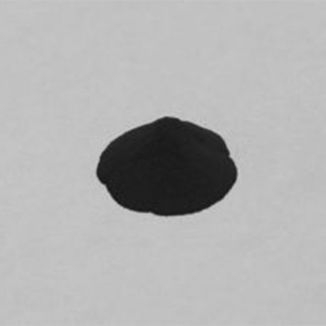 View larger
CIGS | Cu.InxGa1-xSe2
HTHP651
New product
CIGS Cu(In,Ga)Se2 semiconductor material is supplied for thin-film photovoltaic, electronic and research applications. Custom composition, purity, target or powder form, dimensions and documentation are available.
Please contact us if you need customized services. We will contact you with the price and availability in 24 hours.
Data sheet
| Symbol | Cu.InxGa1-xSe2 |
| Purity | 99.99%-99.999% (4N-5N) |
| Size | lump |
| Product | CIGS |
| CAS | NA |
More info
CIGS | Cu.InxGa1-xSe2 Selection Notes
CIGS material is selected by Cu/In/Ga/Se ratio, purity, form, particle size or target dimensions, density and deposition process.
Related Materials and Product Forms
Review Semiconductor Materials, all products and the materials blog.
FAQ
What should be included in a quote request? Specify composition, purity, form, particle size or dimensions, density, backing plate needs, process and quantity.
Can specifications and packaging be customized? Yes. Share technical requirements, quantity, documentation and packaging needs.
High-purity and ultra-high purity CIGS (Cu.InxGa1-xSe2) materials are crucial components for the research, development, and production of advanced technologies which require optimum properties, performance, and quality.
Copper indium gallium (di)selenide (CIGS) is a I-III-VI2 semiconductor material composed of copper, indium, gallium, and selenium. The material is a solid solution of copper indium selenide (often abbreviated "CIS") and copper gallium selenide. It has a chemical formula of CuIn(1-x)Ga(x)Se2 where the value of x can vary from 0 (pure copper indium selenide) to 1 (pure copper gallium selenide). CIGS is a tetrahedrally bonded semiconductor, with the chalcopyrite crystal structure, and a bandgap varying continuously with x from about 1.0 eV (for copper indium selenide) to about 1.7 eV (for copper gallium selenide).
It is best known as the material for CIGS solar cells a thin-film technology used in the photovoltaic industry. In this role, CIGS has the advantage of being able to be deposited on flexible substrate materials, producing highly flexible, lightweight solar panels. Improvements in efficiency have made CIGS an established technology among alternative cell materials.
Usage:
It is crucial a component for the research, development, and production of advanced technologies.
Packing:
It is packed with dacron film, then covered with a sealed plastic film bag or in a polyethylene bottle.
Specifications and Ordering
Specify composition, purity, form, particle size or dimensions, density, backing plate needs, process and quantity.
Applications
Thin-film photovoltaics, semiconductor research, electronic films and PVD development.
Packaging and Custom Options
Materials are supplied in protective packaging appropriate to the product form, with custom dimensions, quantities and documentation available on request.
Inquiry to Heeger Materials
Items marked with an asterisk (*) are required.
Heeger Materials respects your privacy, and we will NOT sell or provide your personal data to other third parties, or allow them to use your personal data for their own purposes. However, we would like to send you information from time to time by mail or email about our products and special offers in addition to the interest categories you've selected above. Read our Privacy Policy
30 other products in the same category:
-
Copper (I)...
-
Germanium...
-
Copper...
-
Copper...
-
Zinc...
-
Tin (II)...
-
Germanium(I...
-
Cadmium...
-
Bismuth...
-
Gallium...
-
Arsenium...
-
Antimony...
-
Indium(III)...
-
Bismuth...
-
Gallium...
-
Arsenium...
-
Antimony...
-
Indium...
-
Zinc...
-
Bismuth...
-
Gallium...
-
Indium...
-
Gallium...
-
Indium...
-
Lead...
-
Zinc...
-
Indium...
-
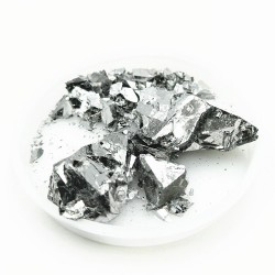
Bismuth...
-
Cadmium...
-
Lead...